
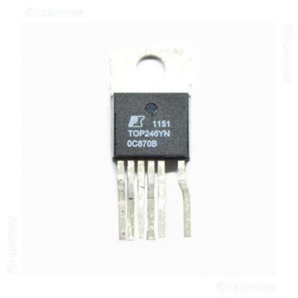
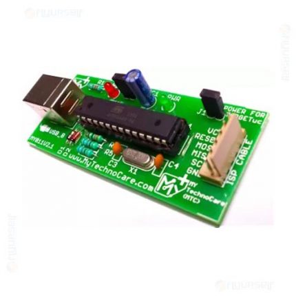
Power Integrations’ TOPSwitch-GX series employs the same tried-and-true TOPSwitch structure. This switcher IC is made up of a single CMOS chip that has a high-voltage 700V power MOSFET, PWM control, fault protection, and other control circuitry. This IC has a number of novel capabilities that help to lower system costs while also improving design flexibility, performance, and energy efficiency.
The typical TOPSwitch DRAIN, SOURCE, and CONTROL terminals are extended by 1 or 3 pins, depending on the package type. The typical TOPSwitch DRAIN, SOURCE, and CONTROL terminals are extended by 1 or 3 pins, depending on the package type. As a consequence, features like line detection (OV/UV, line feed-forward/DCMAX reduction), precise externally set current limit, and remote ON/OFF are available. It also features frequency selection (132 kHz/66 kHz) and may be externally synchronised to a lower frequency.
All package options include soft-start, 132 kHz switching frequency (automatically reduced at light load), and frequency jittering for decreased EMI. Larger creepage packages, a wider DCMAX, and hysteretic thermal shutdown are also provided. Furthermore, all necessary parameters such as current limit, frequency, and PWM gain offers better temperature and absolute tolerances, making design easier and reducing system costs.
This IC is a switched-mode power supply device that transforms a control input current to a duty cycle at the open-drain output of a high voltage power MOSFET. During normal IC operation, the duty cycle of power MOSFETs falls linearly with rising CONTROL pin current.
APPLICATIONS:
- A High Efficiency, 35 W, Dual Output – Universal Input Power Supply
- High Efficiency, 150 W, 250-380 VDC Input Power Supply
- A Universal Input Power Supply with a High Efficiency of 20 W Continuous – 80 W Peak.
- Universal Input Power Supply, 65 W, High Efficiency


Reviews
There are no reviews yet.